HOME » OCXO » OCXO 10 MHz CMOS B 3.3 VOLT 25x25x13 mm B

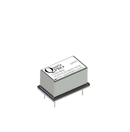
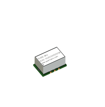
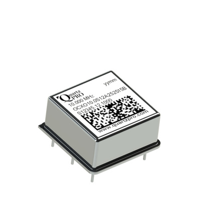
OCXO 10 MHz CMOS B 3.3 VOLT 25x25x13 mm B

No price
Stock status: 0pcs
Hermetically sealed oscillator for best environmental immunity. Wide temperature range. Low close in Phase Noise. Voltage controlled input for external control of output frequency. Low aging in combination with tight temperature stability.

Description

Specification for OCXO Part # OCXO10.0C33B252513B     Download datasheet


1. POWER SUPPLY CHARACTERISTICS (pin 5)

Item

Parameter

Condition

Min.

Typ.

Max.

Unit

Note

1.1

Supply voltage input


3.135

3.3

3.456

V


1.2

Supply current at power on

at 25˚C


1000 /
3.5

mA /
W


1.3

Supply current at steady state

at 25˚C


450 /
1.6

mA /
W

In still air 5 min after power on

1.4

Supply current at steady state

at Min T


mA /
W

In still air 5 min after power on

1.5

Supply current at steady state

at Max T


mA /
W

In still air 5 min after power on


2. CONTROL VOLTAGE INPUT (pin 3)

2.1

Transfer slope


Positive


2.2

Input impedance

100 


kohm


2.3

Min frequency

@ Vc min

-2.4   

-0.8 

ppm

Vc min = 0V

2.4

Nom frequency

@ Vc nom

-200


+200 

ppb

Vc nom = 2.0 V

2.5

Max frequency

@ Vc max

+0.8 


+2.4 

ppm

Vc max = 4.0 V

2.6

Tuning sensitivity


1.5 


ppb/mV


2.7

Tuning linearity


 -10


+10 

%

Deviation from a straight line fit


3. TEMPERATURE 


Min T


Max T


3.1

Temperature range

operating

 -40


+85


Deg C

3.2

Temperature range

storage

-55


+105


Deg C


OCXO 10 MHz CMOS 3.3 VOLT 25x25x13 mm

10MHz OCXO 
Oven Controlled Crystal Oscillator. 
Dimensions in mm


4A. OUTPUT SIGNAL FOR HCMOS, LVCMOS, CMOS (pin 4)

Item

Parameter

Condition

Min.

Typ.

Max.

Unit

Note

4.1

Load


15


pF


4.2

Output Level

VOH / VOL

> 2.4


< 0.3

V


4.3

Duty Cycle


45


55

%


4.4

Rise / Fall time


< 5.0

ns


4B. OUTPUT SIGNAL FOR SINEWAVE (pin 4)

4.5

Output Level

Sinewave


dBm

Load 50 ohm

4.6

Harmonics


dBc


4.7

Non harmonics


dBc


4.8 Short term stability Frequency domain, Phase Noise L(f)

4.8.1

Phase Noise @ offset frequency

1 Hz


 -90

dBc / Hz

1 h after power on and still air

4.8.2

Phase Noise @ offset frequency

10 Hz


-120

dBc / Hz

1 h after power on and still air

4.8.3

Phase Noise @ offset frequency

100 Hz


-140

dBc / Hz

1 h after power on and still air

4.8.4

Phase Noise @ offset frequency

1KHz


-145

dBc / Hz

1 h after power on and still air

4.8.5

Phase Noise @ offset frequency

10KHz


-150

dBc / Hz

1 h after power on and still air

4.8.6

Phase Noise @ offset frequency

100KHz


-155

dBc / Hz

1 h after power on and still air

4.9 Short term stability Time domain, Allan Deviation sy(t)

4.9.1

Sample time (t)

0,1s


1 h after power on and still air

4.9.2

Sample time (t)

1.0s


< 5.E-11


1 h after power on and still air

4.9.3

Sample time (t)

10s


1 h after power on and still air

4.9.4

Sample time (t)

100s


1 h after power on and still air


5. FREQUENCY CHARACTERISTICS

5.1

Stability vs temperature

Min T/ Max T

-8


+8

ppb p-p

External Vc connected

5.2

Calibration accuracy

at 25˚C and Vc nom

-200


+200

ppb

At delivery, 30 min after power ON

5.3

Frequency retrace *

15 min after Power On

 -10


+10 

ppb

Value 30 min after power ON compared to frequency prior to power OFF

5.4

Warm up time

at Vc Nom and 25˚C


5

min

< ±10 ppb from final freq. after PO for 1hour

5.5

Long term stability (aging)

Per day

-0.5


+0.5

ppb

After 30 days of continues operation At 25˚C

5.6

Long term stability (aging)

First year

-100


+100

ppb

After 30 days of continues operation At 25˚C

5.7

Long term stability (aging)

After first year

-40


+40 

ppb

After 30 days of continues operation At 25˚C

5.8

Start up time

At 25˚C and Vc nom


s

From power on to 67 % of V out

5.9

Load change

Cl ± 5%

-1.0


+1.0

ppb


5.10

Vcc change

Vcc ± 5%

-1.0


+1.0

ppb


* Retrace test precondition Power ON 24 h Power OFF 24 h and Vc nom and 25˚C.


6A. REFERENCE VOLTAGE 

6.1

Reference Voltage


V


6B. OVEN ALARM

6.2

High level


V

Oven is ready (steady state)

6.3

Low level


V

Oven is warming up

Datasheet

Document (1)

Specifications

Partno: OCXO10.0C33B252513B
Stock status: 0pcs

Reviews

Add review
Rating (0)
Other products from the same category
  • Small SMD oscillator with 6 pads. Wide temperature range. Fixed frequency output.
    0pcs
    Partno: OCXO40.0C33A151007B
    No price
  • Hermetically sealed ocxo for best environmental immunity. Wide temperature range. Fixed frequency output. Low close in Phase Noise.
    0pcs
    Partno: OCXO10.0C12A252513B
    No price
  • Hermetically sealed oscillator for best environmental immunity. Wide temperature range. Low close in Phase Noise. Voltage controlled input for external control of output frequency. Low aging in com...
    0pcs
    Partno: OCXO10.0S12A362713B
    No price
  • Hermetically sealed oscillator for best environmental immunity. Wide temperature range. Fixed frequency output.
    0pcs
    Partno: OCXO12.8L33A362713B
    No price